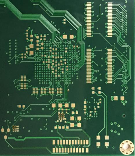
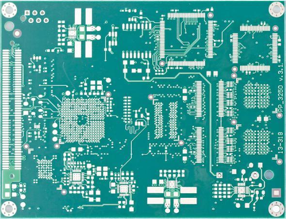
Description
Welcome to Well-Tech - one of the leading manufacturers and suppliers of PCB products in China. Our factory is engaged in PCB manufacturing and offering customized multilayer impedance controlled rigid pcb with minimum trace width and gap at competitive price. High reliability, strong diversity and expert advice are our characteristics. Please contact us if you have inquiry.
Impedance controlled PCB: Impedance is the sum of the resistance and reactance of an electrical circuit expressed in Ohms. In many cases merely by using software models to determine the anticipated impedance with particular dielectric materials and spacing, and then following these request parameters to fabrication.
Layers: 12
Material /Laminate: FR4 TG170
Minimum trace width/gap: 3.5/3.5mil
Board thickness: 1.6mm
Copper weight: inner 0.5oz & outer 1oz
Finishing: ENIG
|
The typical tolerance for impedance result is +/- 10%. |
|
1) H is the height of the dielectric. It changed in steps. Dielectric thickness change +/- 1 mil which affect impedance results in +/- 2 ohms. |
|
2) Er is the dielectric of the material. Having a good idea of the Er is necessary since +/- 0.1 Er results in +/- 0.5 Ohms. |
|
3) W is the trace width. S is the trace separation. Typical W and S change +/-2 mil which affect impedance results in about +/- 2 ohms. Typical the W2=W1-0.5 |
|
4) T is the trace copper thickness. Due to outer layer traces need plating, and linear tolerance is 20%, this affect impedance results in an uncertainty of +/-0.2 ohms. |
|
5) C is the parameter for solder mask coating. Typical coating thickness and dielectric constant should be considered into calculation since it will affect the results in about +/- 2 or 3 ohms. And the Er range is 3.4~3.8. |


